Sometimes the PIC is a part of the schematic and thus of the Printed
Circuit Board (PCB) but, in other projects, the PIC is wired on a
"stand alone" development board connected to the controlled device
by several lines.
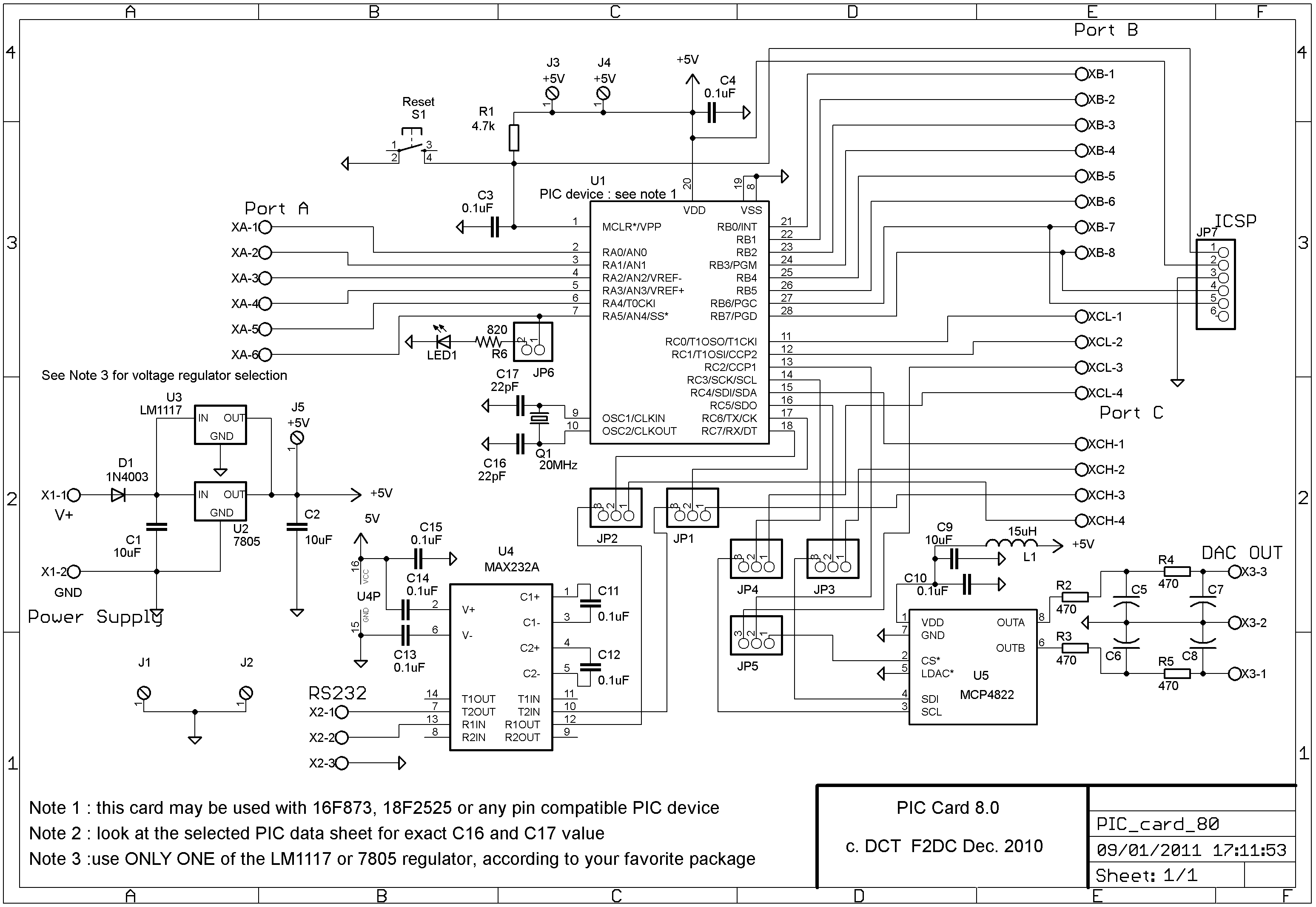
Over the years I used 16F84, 16F628, 16F873/876,
18F252, 18F2525... microcontrollers and developed several PCBs
for these chips.
Some of you asked me for the schematics, so I present here these home made development boards.
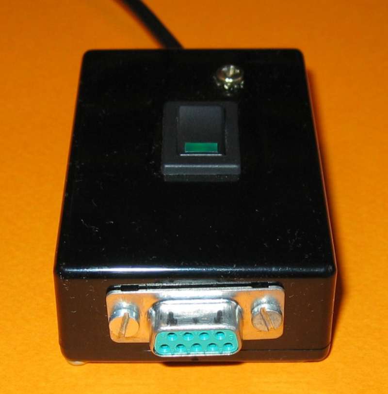
Here are some pictures of the card, the first one with a 7805 voltage regulator, the 2nd and 3rd using a LM1117 SMD regulator located on the solder side .
Card with a 7805 regulator on the components side Card with a LM1117 SMD regulator on the solder side (lower right corner)
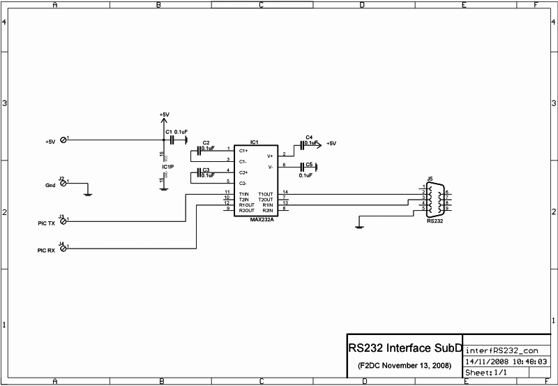
Click on the picture to enlarge the schematic.
You may download the PCB artwork (zip file of the 2 sides) as well as the components layout

Note : the above PCB has been made by FAR CIRCUITS.
- The User Manual is available : Click here to download this 500 kbytes PDF file
Software : a demo "LED18F2525.hex" program blinking the onboard LED and "SPI_ramp4822.hex" generating sawtooth signals on the D/A converter output pins are available. These programs are designed for use with a PIC 18F2525 running at 20 MHz.
Click here to download these 2 hex files.
A picture of the dual ramp signals is shown below.

Note : I can provide interested readers with the C source code of these programs. However, they are written with the CCS compiler and I can't say anything about their compatibility with other compilers.
This
card is easier to build because it is a one-sided PCB, the ground
plane being the upper side of the PCB. There are no provision
for D/A converter or ICSP connection.
A RS232 link is available thanks to the MAX232A interface, but may be omitted if not needed.
Many terminal posts are available to connect the A, B and C ports to the external world.
The card is powered by any DC voltage greater than 8 Volts, a 7805 regulator associated with a foolproof diode providing the needed 5 Volts power supply.

Note
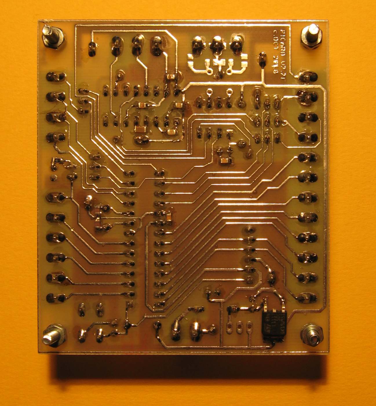
: This circuit is built on a dual sided PCB, the upper (components)
side remaining unetched while the lower (solder) side is etched using
the above mentioned artwork : the upper side is thus the ground plane.
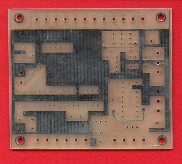
As most of the components pins must be insulated from this ground
plane, I use a large drill (6 mm or more) to remove copper around holes
not connected to ground. The photo below is a close-up of two insulated
holes (upper part of the picture) and a grounded hole (lower part).