Some DDS circuits developed here, just for history !
(updated January 30, 2025)
Direct Digital Synthesis (DDS) is an attractive method to generate stable signals having good spectral purity and fast frequency settling time.
You'll find a lot of information on the DDS theory and implementation in an article published by my son Lionel in the "IEEE Signal Processing Magazine" you can download from his WEB page :
http://lionel.cordesses.free.fr/gpages/electronics.html
- More information on the subject is also available in the chapter 21 of the book "Streamlining Digital Processing" Click here
- Furthermore, have a look at the Wikipedia page devoted to the DDS.
At
the beginning of the 1990s, Lionel and I built from scratch a home made
DDS (picture below) generating signals in the audio range.

I
have used many different DDS chips since then, mainly from Analog
Devices, to build signal generators for different purposes and I
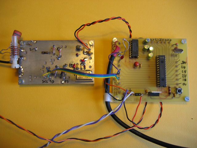
present some of them below. 1. AD9834 board.
The
AD9834 is a low cost, low-power DDS ( a few mA at 5V) that can be
clocked up to 50 MHz. It is housed in a 20 lead TSSOP SMD package.
I designed a PC board that can be used as a simple DDS
development tool when associated with a PIC 16F873 microcontroler card
described elsewhere.
- Click here to get the schematic diagram of the DDS unit
The PCB artwork of the lower side (solder side) is available as a PDF file by clicking here.
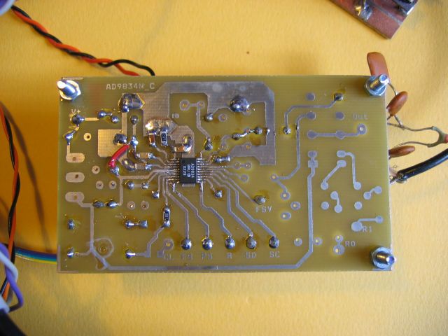
The
upper side of the PCB remains unetched : it is used as a ground plane
to which all ground connexions are soldered. The AD9834 chip is
soldered on the lower side, the other components being on the upper
side.
It is necessary to remove the unetched copper around the
components holes not connected to ground. I use a 6 to 8 mm drill
to do that.
One can see some of these "insulated holes" on the picture below showing the complete DDS card .
Some remarks :
- Any clock oscillator up to 50 MHz can be used.
-
There are two 5 V regulators on the card , one for the digital power
supply and the other for the analog supply. You can use only one
if high spectral purity is not a matter of great concern.
- The output relay allowing selection of sine/triangle or square waveform can be omitted if not necessary.
-
The inductor on the left of the PCB (picture below) is a
part of the elliptic low-pass filter rejecting the DDS clock frequency.
Such filters can be designed with the help of filter tables in
the Zverev's "Handbook of Filter Synthesis" (or in the much less
expensive "ARRL Handbook").
- The SCLK DDS pin is connected to port B5 of the PIC, the SDAT to line B4 and FSYNC to line B2.
- Pins PhSEL and FSEL are grounded if not used.
The PIC software controlling the DDS is written in C language using a CCS compiler.
A demo program (in CCS C language) showing how to send words from
the PIC to the DDS registers is available : it generates a 18.1125 MHz
signal but may be modified to create any other frequency inside the
AD9834 range. Click here to get this file.
The
picture on the left below shows the DDS board connected to the PIC
board and on the right is a bottom view, the DDS being the
small SMD chip .


Click here to get the schematic diagram of the PIC card.
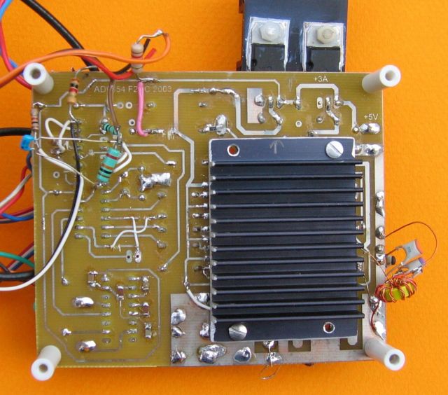
2.AD9854 board.
Some years ago I
needed an RF source and selected the AD9854 because of its high
upper frequency limit. In contrast to the AD9834 it is a power
hungry device ( # 500 mA at 3.3 V) and the heat sink is a must.
This chip is a large one (80 pins LQFP SMD package) and is not so easy
to solder on the PCB!
The schematic is available here
Remarks :
- The AD9854 is under control of a PIC 18F2525 included on the PCB. The control interface I select is the 3 wires serial SPI.
- A rotary encoder connected to pins
B6 and B7 of the PIC allows frequency tuning and a 3
position switch controls frequency step.
- There are 2 output lines,
one in phase and the other in quadrature, each connected to the DDS
output pins through elliptic low-pass filters.
- Two clock modes are available
: direct or multiplied. While a lower clock oscillator can be
used when the second mode is selected, the output
spectrum is not as clean : I thus used the first
method.
- DDS
supply voltage is 3.3 V and the PIC one 5 V : resistive voltage
dividers take care of the control lines going from the PIC to the
DDS.
- Prog 2 terminal (connected to pin B5) is used only during the software development cycle.
- The PIC code was developed with the aforementioned CCS C Compiler.
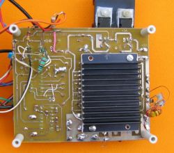
Below are two pictures of the card,
the left one showing the top side and the right one the bottom side.
The large black heat sink on the right of the picture is the power
dissipation device for the AD9854 hidden under from sight.
Note
: This method allows proper cooling of the DDS chip
under operating conditions in use here : 100 MHz clock, no
Sinc and no Digital Multiplier engaged. Be careful in case
of harder operating modes!!!

The PCB shown on these pictures is the
first one I designed and some changes or improvements have been
introduced during the tests.
The PCB artwork and part placement files are available.
Click here to download.
This new design is slightly different from the one shown on the above pictures.
Home