The story.
The first step was to get the PCB : I sent an Email to Ivan Makarov VE3IVM
who designed a PCB including the N2PK modifications for dual fast
ADCs. A few days later, I received an envelope with three
beautiful PCBs (the VNA and two coupler boards).
I
then ordered the Valpey-Fisher oscillator to Eugene Skopal AE2F
and most of the passive and active components to Digikey.
I was now ready to build the VNA.
As components
are SMDs, one must be careful when soldering them on the board : I
used the SMD Holding Device described elsewhere in my Web pages and, to mitigate mistakes, I double checked each component before soldering it.
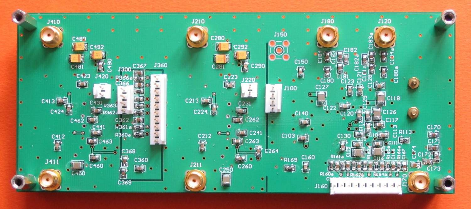
In a short time, the main board was ready and checked. Both sides of the populated PCB are shown below (click on the pictures to enlarge) :
I then designed a power supply around a DATEL DC/DC converter : this converter is oversized (5 V @ 3 A and 12 V @ 500 mA) for sure,
but it was in my junk box! A long time burn-in was then
performed, the power supply outputs being connected to wire wound
resistors : during this test, I periodically checked the DC output
voltages and watched the noise levels present on these lines.
Measured overall efficiency was around 80%.
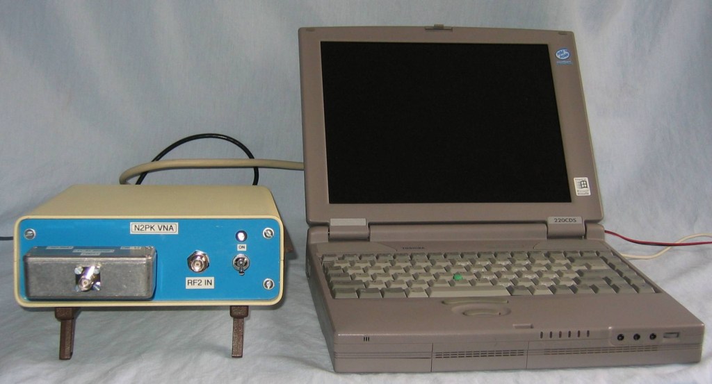
After that, I put the VNA, the power supply and the connectors up on a temporary plywood base, in order to make measurements easier during the first tests.
Well, everything was now ready for the smoke test!
I
carefully followed the N2PK's and VE3IVM's advice, checking voltages on
several test points of the VNA board, and was very pleased to
read nominal values everywhere.
After connecting the VNA to the parallel port of my PC, I ran one of the N2PK debug programs and was able to talk to the VNA!
Now,
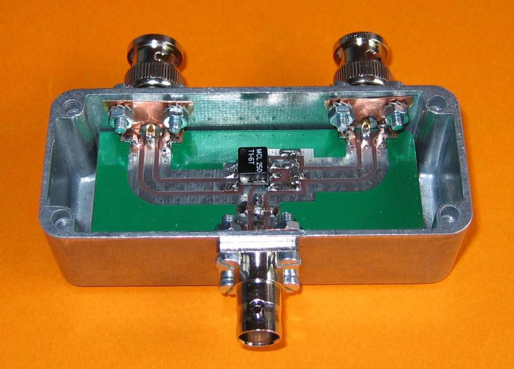
it was time to build the BNC Open and Short calibration standards,
and the T1-6T reflexion bridge on one the two boards provided by
VE3IVM : this coupler is shown below.
Tests
of the VNA associated with the coupler, on several known loads, were
then successfully conducted, and results were in good agreement with
values measured with an HP analyzer.
Before
installing my VNA in a convenient enclosure, I fastened a home made
heatsink over the DDSs and the time base, using the two holes intended
for that purpose on the PCB . I was greatly inspired by the VE3FJ
method.
The
enclosure for this equipment is a metal box I had in my junk box : the
pictures below shows that this new job suits it perfectly.
Top view

Front panel with the T1-6T coupler

Rear panel
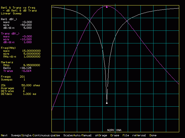
Here is a sample picture of measurement carried out on a simple RLC circuit resonating around 9 MHz (N2PK software) :
Conclusion.
This is the end of the building phase and the beginning of other adventures in the world of impedance measurement.
I want to sincerely thank Paul N2PK, Ivan VE3IVM and all people involved in the development of this project (software as well as hardware).Congratulations to all!


